1 / 1
china electronic pcb manufacture
Get Latest Price
Send Inquiry
| Model No. : | Pcba Service |
|---|---|
| Brand Name : | OEM |
OurPCB Tech. Ltd
You might also like
Product description
Product Description 1.PCB Board Processing Capability:
Product Descriptions ♦ All of the above description is to demonstrate the ability of our factory, if you have specific requirements, please contact us. 2.Detailed Terms for PCB Assembly:
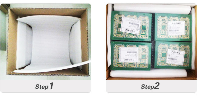
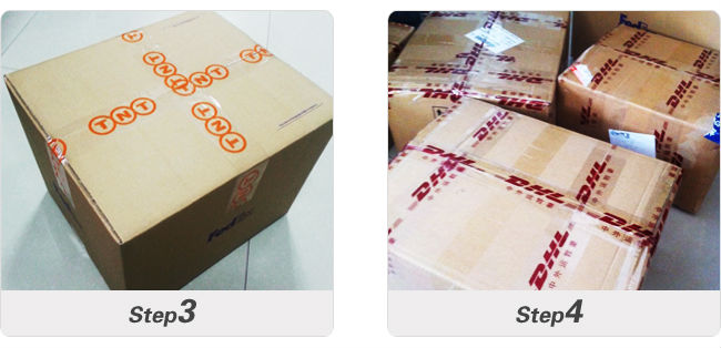
PCBA Produc Line:  Technical characteri Dielectiric strength:2.5kv dc-2seconds Conductor resistance:Max 9.38ohm/100m at 20°C Max ring resistance:16.8ohm/100m at 20°C Max mutual capacitance:530pf/100m Max capacity unbalance:110pf/100m Impedance:100±15%ohm at 1-250MHZ resistance:16.8 ohm/100m at 20°C Operating tempetature: -20°C~+70°C Packaging & Shipping


| 1 | Layers | Single Sided, 2 to 36 Layer |
| 2 | Board material type | FR4 |
| 3 | Compound material lamination | 4 to 6 layers |
| 4 | Copper Thickness: | 1oz |
| 5 | Board Thickness: | 1.6mm |
| 6 | Min. Hole Diameter: | 0.15mm |
| 7 | Min. Line Width: | 0.1mm |
| 8 | Min. Line Spacing: | 0.1mm |
| 9 | Surface Finishing: | HASL lead free |
| 10 | Solder mask: | Green |
| 11 | Outer layer copper thickness | 8.75 to 175µm |
| 12 | Inner layer copper thickness | 17.5 to 175µm |
| 13 | Drilling hole diameter (mechanical drill) | 0.25 to 6.00mm |
| 14 | Finished hole diameter (mechanical drill) | 0.20 to 6.00mm |
| 15 | Hole diameter tolerance (mechanical drill) | 0.05mm |
| 16 | Hole position tolerance (mechanical drill) | 0.075mm |
| 17 | Laser drill hole size | 0.10mm |
| 18 | Board thickness and hole diameter ratio | 10:1 |
| 19 | Solder mask type | Green, Yellow, Black, Purple, Blue, White and Red |
| 20 | Minimum solder mask | Ø0.10mm |
| 21 | Minimum size of solder mask separation ring | 0.05mm |
| 22 | Solder mask oil plug hole diameter | 0.25 to 0.60mm |
| 23 | Impedance control tolerance | ±10% |
| 24 | Surface finish | Hot air level, ENIG, immersion silver, gold plating, immersion tin and gold finger |
| Technical Requirement | Professional Surface-mounting and Through-hole soldering Technology |
| Various sizes like 1206, 0805, 0603 components SMT technology | |
| ICT(In Circuit Test), FCT(Functional Circuit Test) technology | |
| PCB Assembly With UL, CE, FCC, Rohs Approval | |
| Nitrogen gas reflow soldering technology for SMT | |
| High Standard SMT&Solder Assembly Line | |
| High density interconnected board placement technology capacity | |
| Quote&Production Requirement | Gerber File or PCB File for Bare PCB Board Fabrication |
| BOM(Bill of Material) for Assembly, PNP(Pick and Place file) and Components Position also needed in assembly | |
| To reduce the quote time, please provide us the full part number for each components, Quantity per board also the quantity for orders. | |
| Testing Guide&Function Testing method to ensure the quality to reach nearly 0% scrap rate | |
| OEM/ODM/EMS Services | PCBA, PCB assembly: SMT & PTH & BGA |
| PCBA and enclosure design | |
| Components sourcing and purchasing | |
| Quick prototyping | |
| Plastic injection molding | |
| Metal sheet stamping | |
| Final assembly | |
| Test: AOI, In-Circuit Test (ICT), Functional Test (FCT) | |
| Custom clearance for material importing and product exporting | |
| Other PCB Assembly Equipments | SMT Machine: SIEMENS SIPLACE D1/D2 / SIEMENS SIPLACE S20/F4 |
| Reflow Oven: FolunGwin FL-RX860 | |
| Wave Soldering Machine: FolunGwin ADS300 | |
| Automated Optical Inspection (AOI): Aleader ALD-H-350B,X-RAY Testing Service | |
Fully Automatic SMT Stencil Printer: FolunGwin Win-5 |
 Technical characteri Dielectiric strength:2.5kv dc-2seconds Conductor resistance:Max 9.38ohm/100m at 20°C Max ring resistance:16.8ohm/100m at 20°C Max mutual capacitance:530pf/100m Max capacity unbalance:110pf/100m Impedance:100±15%ohm at 1-250MHZ resistance:16.8 ohm/100m at 20°C Operating tempetature: -20°C~+70°C Packaging & Shipping


Send your inquiry to this supplier
Send Inquiry


