

Sign In Join Free


Video
1 / 4
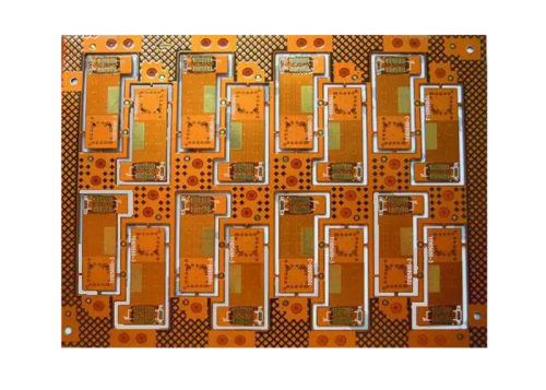
PCB Board Project Copper Clad PCB Board
Options:
- Specification OEM
- Competitive price
- No MOQ
- 24 hours quick turn prototype
- Prototype&mass production
- 100% Electrical test guarantee
| Model No. : | LDJPCB-S9034 |
|---|---|
| place of origin : | China |
Huizhou, Guangdong, China
- Manufacturer
- OEM service
- Gold Supplier

- Platform Certification

- SGS Certification


Product description
Product Description
PCB Board Project Copper Clad PCB Board.Copper PCBs are widely used in outdoor lighting, stage lighting, automotive lighting, violet UV curing equipment, medical equipment, electric power and other fields.
PCB Business:
Lead Time:7-10 days for 2L
10-12 days for 4L
12-15 days for over 6L
Technical Capability:
1.Material:Aluminum,Copper
2.Layer:Single-Sided/Double-sided
3.Board Thickness:0.5-6mm
4.Copper Thickness:35um/70um/105/um/140um/175um/210um/245um/280um/315um
5.Max. Board Size:1500mm*500mm
6.Min.Board Size:5mm*5mm
7.Surface Finshed:HASL/ENIG/OSP/Silvering
8.Line Width/Space:0.1mm/0.1mm
9.Min Punching Hole:Board thickness below 1.0mm,is 1.0mm
10.Min. Punching Square slot:Board thickness below 1.0mm,is 1.0mm*1.0mm
11.Min.Drill Hole Diameter:0.6mm
12.V-cut Degree Tolerance:±5degree
13.V-CUT Board Thickness:0.6mm-4.0mm


PCB&PCBA file requite:
1.Gerber file or Schematic diagram of printed circuit board.
2.Material,Board thickness,Copper thickness and Surface finish of PCB
(please write in Gerber file or send data to us.)
3.BOM (list of components)
4.Number of circuits you need.
Company Information
ABOUT US
Huizhou Liandajin Electronic Co.,Ltd is a solutioner for high precision double-sided and multi-layer printed circuit board.

PCB manufacture workshop
LDJ has 15 years of PCB production experience.Our factory covers more than 20000m2 and the output had reached 500000m2 per month.We had mature production lines,professional production equipments and testing machines.

Founction Test
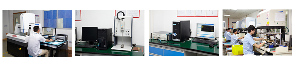

PCB Assembly


In 2015,the company has transferred from a single PCB manufacturer to a one-stop solutioner for PCBA and electronic products by resource integration and huge investment of SMT and X-Ray examing equipment.


CERTIFICATION

APPLICATION USE


Video
Huizhou, Guangdong, China
- Manufacturer
- OEM service
- Gold Supplier
- Platform Certification
- SGS Certification
Send your inquiry to this supplier
Product Alert
Subscribe to your interested keywords. We will send freely the latest and hottest products to your Inbox. Don't miss any trade information.
Your use of this website constitutes acknowledgement and acceptance of our Terms & Conditions.
Copyright © 2009-2024 Bossgoo Co., Ltd. All rights reserved.
