1 / 1
Hall Effect Current Sensor
Options:
| Model No. : | THB-DS3S6 |
|---|---|
| place of origin : | China |
Zibo, Shandong, China
- Distributor/Wholesaler
- Gold Supplier

- Platform Certification


Product description
|
Product introduction: |
Application: |
|
Ø Single power supply: +3.3v DC Ø Customized according to requirements; Ø Both perforation and PCB measurement; Ø Hall effect principle - closed loop current sensor; Ø The output is a voltage signal with polarity and no negative value; Ø It can measure the current of DC, AC, pulse and various irregular waveforms under the condition of electrical isolation; |
Ø Application on Inverter Ø Standard battery monitoring Ø Variable speed drive applications Ø UPS uninterruptible power supply Ø Solar power management system Ø Drive control of variable frequency household appliances |
Electrical characteristics:
|
Parameter |
Symbol |
THB06DS3S6 |
THB15DS3S6 |
THB25DS3S6 |
THB50DS3S6 |
|
Rated current |
IPN(A) |
06 |
15 |
25 |
50 |
|
Measuring range |
IP(A) |
0~±12 |
0~±30 |
0~±50 |
0~±100 |
|
Measure resistance |
RM(Ω) |
100±0.1% |
50±0.1% |
25±0.1% |
25±0.1% |
|
Sensitivity |
G(mA/A) |
104.16 |
41.67 |
25 |
12.5 |
|
Output voltage |
VO(V) |
1.65±0.625*(IP/IPN) |
|||
|
Working power supply |
VC(V) |
+3.3V DC±5% |
|||
|
Insulation voltage |
VD(V) |
50/60Hz,1min,4kV;RMS |
|||
|
lightning surge |
Vw(V) |
@ at1.2/50µs,>8.0kV |
|||
|
Output load capacitance |
CL(nF) |
<10nF @Vo~GND |
|||
General parameters:
|
Project |
Condition |
Date |
Unit |
|
Accuracy XG |
@ IPN,T=25℃ |
<±0.7 |
% |
|
Zero offset voltage VOE |
@ IP=0,T=25℃ |
<±20 |
mV |
|
Current offset temperature drift VOT |
@ IP=0,-40~+85℃ |
<±0.5 |
mV/℃ |
|
Linearity εr |
|
≤0.1 |
%FS |
|
Follow accuracy di/dt |
|
>50 |
A/µs |
|
Response time tra |
@ 90% of IPN |
<1.0 |
µs |
|
Operating bandwidth BW |
-1dB |
DC-200 |
kHZ |
|
Creepage distance dcp |
Shell surface |
15.4 |
mm |
|
Working temperature TA |
|
-40~+85 |
℃ |
|
Storage temperature TS |
|
-55~+125 |
℃ |
|
Static power consumption IC |
|
10+Is |
mA |
|
Secondary pin mounting hole size |
(+,0,OUT) |
>1.1 |
mm |
|
Primary pin mounting hole size |
1,2,3,4,5,6 |
>1.5 |
mm |
|
Product weight m |
|
10 |
g |
|
Shell material |
PBT material containing 30% glass fiber,Flame retardant grade:UL94- V0; |
||
|
Standard |
IEC60950-1:2001 EN50178:1998 SJ20790-2000 |
||
Structural drawing: (mm)

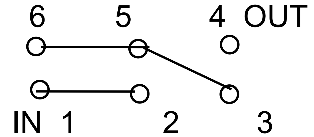
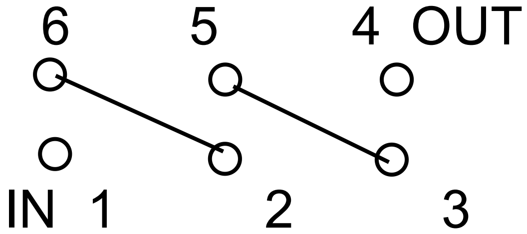
Connection diagram:
|
Primary wire turn |
Primary rated current (A) |
Output voltage (V) |
Primary resistance (mΩ) |
Primary inductance (µH) |
Enter PIN connection |
|
1 |
±6 (±15,±25,±50) |
1.65±0.625 |
0.18 |
0.013 |

|
|
2 |
±3 (±7.5,±12.5,±25) |
1.65±0.625 |
0.81 |
0.05 |

|
|
3 |
±2(±5,±8.3, ±16.6) |
1.65±0.625 |
1.62 |
0.12 |

|
This product has two input methods:
1) Cable perforation input; 2) PCB input mode;
Suitable current input mode can be selected according to needs;
A: For the cable current input mode, the cable should pass through the hole of the Hall current sensor;
Take thb06ds3s6 as an example. If the perforation of the cable is 1 turn, the rated current is 6A; if the perforation of the cable is 2 or 3 turns, the rated current is 3A or 2A; If you follow this input method, please do not use PCB input method at the same time;
B: For PCB input mode, the input turns and rated input current parameters are determined according to the connection mode of the input pin.
There are three ways to input pin: 1t, 2T, 3T; The corresponding input rated current is: 6a, 3a, 2A; See wiring diagram for specific connection mode; When using this method, do not use the perforation input method at the same time;
Relationship between input current and output voltage:
Taking THB25DS3S6 as an example, the relationship between input current and output voltage is shown in Table 1 and Fig.1 below
Table 1:
|
Input current(A) |
-50 |
-25 |
0 |
25 |
50 |
|
Output voltage (V) |
0.4 |
1.025 |
1.65 |
2.275 |
2.9 |

Fig. 1 Relation between the input current (DC) and output voltage (DC)
Remarks:
1. Connect the current according to the calibrated direction of the wiring diagram; Pay attention to the positive and negative current;
2. Wiring according to the definition of the calibrated functional pin in the structure diagram;
3. The temperature of primary conductor shall not exceed 100 ℃;
4. When the busbar should be fully filled with primary perforation, the dynamic response and di/dt follow-up accuracy are the best;
5. The above specifications are calibration specifications, and our company can customize products according to customers' requirements.
6. If there are new changes in our products, please do not notice, and the actual product parameters shall prevail;
Zibo, Shandong, China
- Distributor/Wholesaler
- Gold Supplier

- Platform Certification

Send your inquiry to this supplier


